Ask an Expert
Planning the right solution requires an understanding of your project and system requirements. Let Kingston's experts guide you.

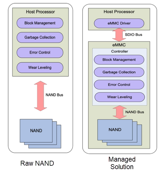
NAND Flash storage is not a simple read/write data medium. For reliable use, several algorithms should be implemented: NAND block management, garbage collection, error control, and wear leveling. Modern NAND Flash is managed, with algorithms on the storage device, not implemented in the host processor. This is to the benefit of its users, as it makes NAND management less complex for the host and simplifies product support and sustainment.
Host writes to NAND Flash have inefficiencies that can cause the medium to fail earlier. NAND’s smallest organizational unit is the page, which can be read and programmed but not erased. The only organizational unit which can be erased is the block, which consists of many pages. Therefore, pages cannot be overwritten until a block is erased. Blocks can over time fail as their endurance level is reached. Defects leading to early failures can also occur.
NAND Flash has limited program-erase cycles available. Reaching that limit means the device is in EoL state, meaning that it is no longer reliable. Endurance varies depending on the NAND cells’ configuration.
Single Level Cell configuration: this setup has the highest endurance and the greatest margin of error.
|
eMMC LBA 512B Sector Address |
NAND Page & Block Address |
| 0:31 | Blk10, Pg101 |
| 32:63 | Blk10, Pg102 |
| 64:95 | Blk10, Pg103 |
| 96:127 | Blk10, Pg104 |
| 128:159 | Blk15, Pg57 |
| 160:191 | Blk8, Pg129 |
| 192:223 | Blk10, Pg107 |
| 224:255 | Blk22, Pg88 |
eMMC reads and writes to 512-byte sector units, which are logical, not physical. Sector addresses are called Logical Block Addresses, or LBAs. When data is modified, erasing the entire NAND block is impractical, causing inefficient wear on pages that did not change. An LBA-PBA (Physical Block Address) mapping scheme provides smaller writes to balance block wear, a practice called wear leveling. By means of an address translation table, LBAs are mapped to PBAs. This process balances block wear and improves write speed.
The process of address mapping works as follows:
Small, random, non-page aligned rewrites are usually the greatest source of write amplification. To minimize WAF, writes should be aligned on a page boundary in multiples of page size units. This optimal unit size is in the Optimal Write Size field of the Extended CSD register.
The formula for determining Total Bytes Written, or TBW, is straightforward:
Often, WAF is between 4 and 8, but it depends on the host system write behavior. For example, large sequential writes produce a lower WAF, while random writes of small data blocks produce a higher WAF. This kind of behavior can often lead to early failure of storage devices.
For example, a 4GB eMMC with an endurance factor of 3000 and a WAF of 8 will equate to:
The Total Bytes Written of the eMMC device is 1.5TB. Therefore, we can write 1.5TB of data over the lifecycle of the product before reaching its EoL state.
To estimate your TBW requirements, estimate the daily usage of the device in question. For example, a workload featuring 500MB of daily write usage (and an intended 5 year lifecycle) will need a device that can reach a TBW greater than 915GB:
The TBW can be used to determine the maximum permissible WAF for a device, since TBW = (DC * EF) / WAF. If your device life cannot reach the target TBW for your product application, you can try to improve it. Consider putting it in Pseudo Single Level Cell mode, which can increase endurance tenfold by converting the device from TLC or MLC to single-bit-per-cell mode. However, this drastically reduces capacity: 50% for a two-bit-per-cell MLC device, and over 66% for a three-bit TLC device. If this solution is unsatisfactory for you, choosing a larger device to handle the same workload also helps. A device with twice the capacity will have double the TBW.
Kingston’s eMMC algorithms achieve a low write amplification factor. We offer multiple configurations to balance performance, lifetime, and reliability. Device age can be monitored by using the JEDEC lifetime estimate tools filed in the EXT_CSD, a feature shared with all eMMC devices. Life is reported at increments of 10% based on the device’s endurance. One tool reports the age of TLC or MLC-configured NAND Flash blocks, while the other reports the age of blocks configured in pseudo-SLC mode. Kingston eMMC devices also have vendor commands to return the average block age of the device. These are more precise than the JEDEC tools but require a little software development to use. Alternatively, you can send your aged device to Kingston for more comprehensive analysis.
#KingstonIsWithYou

Planning the right solution requires an understanding of your project and system requirements. Let Kingston's experts guide you.

Product longevity is a key concern for many embedded applications that typically require a lifetime of 7-10 years. Given the fast pace at which technology is advancing and changing, long term sustainment of embedded products can be challenging.

It's important to understand how the NAND flash on eMMC is being managed in modern devices and how that relates to its life cycle. This guide will help designers and engineers understand how to estimate and validate the useable life of an eMMC storage device in their system design.

SNUC Systems, a manufacturer specializing in compact and rugged technology, partners with Kingston Technology to supply components for their products.

Premio Inc makes rugged computing solutions for industrial use, partnered with Kingston.

There are many features in Kingston’s Industrial cards like Bad Block Management and Wear Leveling.

Learn why Signpost chose Kingston SSD and memory to support their education solutions.

South Seas Data earned its success as a tech services provider with reliable parts from Kingston.

In this eBook, we speak with experts about the journey of data storage, and what the future holds.

Industrial SSD are for industrial system builders. The SSDs go through qualification process so they can be added to system BOM.

Kingston powers WolfVision’s products to bring hybrid meetings to companies and organizations.


